|
|
Tolerance is a critical factor impacting the performance and cost of an
optical system. Optical components usually require much tighter tolerances
than that commonly associated with mechanical components. As a result,
special equipment and techniques are used in the manufacturing and measuring of
the optical tolerances.
Part 1: Optical element tolerances
Jump to part 2: Modulation transfer function (MTF)
- Surface accuracy
-
When attempting to specify how closely an optical surface conforms to its
intended shape, a measure of surface accuracy is needed. Surface accuracy
can be determined by interferometric techniques. Traditional techniques
involve comparing the actual surface to a the test plate gage. In this
approach, surface accuracy is measured by counting the number of rings or
fringes and examining the regularity of the fringe. The accuracy of the fit
between the lens and the test gage (as shown below) is described by the
number of fringes seen when the gage is in contact with the lens. Test
plates are made flat or spherical to within small fractions of a fringe.
Modern techniques for measuring surface accuracy utilize phase measuring
interferometry with advanced computer data analysis software.
During manufacture, a precision component is frequently compared with a test
plate that has an accurate polished surface that is the inverse of the
surface under test. When the two surfaces are brought together and viewed in
nearly monochromatic light, Newton’s rings (interference fringes caused by
the near-surface). The number of rings indicates the difference in radius
between the surfaces. This is known as power or sometimes as figure. It is
measured in rings that are equivalent to half wavelengths. Beyond their
number, the rings may exhibit distortion that indicates non-uniform shape
differences. The distortion may be local to one small area, or it may be in
the form of noncircular fringes over the whole aperture. All such
non-uniformities are known collectively as irregularity.
- Surface flatness
-
Surface flatness is simply surface accuracy with respect to a plane reference
surface. It is used extensively in mirror and optical flat specifications.
- Centration
-
The mechanical axis and optical axis exactly coincide in a perfectly centered
lens. For a simple lens, the optical axis is defined as a straight line that
joins the centers of lens curvature. For a plano-convex or plano-concave lens,
the optical axis is the line through the center of curvature and perpendicular
to the plano surface. The mechanical axis is determined by the way in which the
lens will be mounted during use. There are typically two types of mounting
configurations, edge mounting and surface mounting. With edge mounting, the
mechanical axis is the centerline of the lens mechanical edge. Surface mounting
uses one surface of the lens as the primary stability for lens tip and then
encompasses the lens diameter for centering. The mechanical axis for this type
of mounting is a line perpendicular to the mounting surface and centered on the
entrapment diameter. Ideally, the optical and mechanical axes coincide. The
tolerance on centration is the allowable amount of radial separation of these
two axes, measured at the focal point of the lens. The centration angle is equal
to the inverse tangent of the allowable radial separation divided by the focal
length. Centration error is measured by rotating the lens on its mechanical axis
and observing the orbit of the focal point. To determine the centration error,
the radius of this orbit is divided by the lens focal length and then converted
to an angle.
- Surface quality
-
Cosmetic surface quality describes the level of defects that can be
visually noted on the surface of an optical component. Specifically, it
defines state of polish, freedom from scratches and digs, and edge
treatment of components. These factors are important, not only because
they affect the appearance of the component, but also because they
scatter light, which adversely affects performance. Scattering can be
particularly important in laser applications because of the intensity of
the incident illumination. Unwanted diffraction patterns caused by
scratches can lead to degraded system performance, and scattering of
high-energy laser radiation can cause component damage. Over specifying
cosmetic surface quality, on the other hand, can be costly. The most
common and widely accepted convention for specifying surface quality is
the U.S. Military Surface Quality Specification, MIL-0-13830A, Amendment
3. IMPORTANT: Surface quality can be impacted if improper cleaning
is used.
As stated above, all optics in this catalog are referenced
to MIL-PRF-13830B standards. These standards include scratches, digs,
grayness, edge chips, and cemented interfaces. It is important to note
that inspection of polished optical surfaces for scratches is
accomplished by visual comparison to scratch standards. Thus, it is not
the actual width of the scratch that is ascertained, but the appearance
of the scratch as compared to these standards. A part is rejected if any
scratches exceed the maximum size allowed. Digs, on the other hand,
specified by actual defect size, can be measured quantitatively. Because
of the subjective nature of this examination, it is critical to use
trained inspectors who operate under standardized conditions in order to
achieve consistent results.
The scratch-and-dig designation for a component or
assembly is specified by two numbers. The first defines allowable
maximum scratch visibility, and the second refers to allowable
maximum dig diameter, separated by a hyphen; for example, 80–50
represents a commonly acceptable cosmetic standard. 60–40 represents
an acceptable standard for most scientific research and commercial
applications. 10–5 represents a precise standard for very demanding
laser applications.
SCRATCHES
A scratch is defined as any marking or tearing of a
polished optical surface. In principle, scratch numbers refer to the
width of the reference scratch in ten thousandths of a millimeter.
For example, an 80 scratch is equivalent to an 8-µm standard
scratch. However, this equivalence is determined strictly by visual
comparison, and the appearance of a scratch can depend upon the
component material and the presence of any coatings. Therefore, a
scratch on the test optic that appears equivalent to the 80 standard
scratch is not necessarily 8 µm wide. If maximum visibility
scratches are present (e.g., several 60 scratches on a 60–40 lens),
their combined lengths cannot exceed half of the part diameter. Even
with some maximum visibility scratches present, MIL-0-13830A still
allows many combinations of smaller scratch sizes and lengths on the
polished surface.
DIGS
A dig is a pit or small crater on the polished optical
surface. Digs are defined by their diameters, which are the actual
sizes of the digs in hundredths of a millimeter. The diameter of an
irregularly shaped dig is 1/2#(length plus width): 50 dig = 0.5 mm
in diameter 40 dig = 0.4 mm in diameter 30 dig = 0.3 mm in diameter
20 dig = 0.2 mm in diameter 10 dig = 0.1 mm in diameter. The
permissible number of maximum-size digs shall be one per each 20 mm
of diameter (or fraction thereof) on any single surface. The sum of
the diameters of all digs, as estimated by the inspector, shall not
exceed twice the diameter of the maximum size specified per any
20-mm diameter. Digs less than 25 micrometers are ignored.
EDGE CHIPS
Lens edge chips are allowed only outside the clear
aperture of the lens. The clear aperture is 90% of the lens diameter
unless otherwise specified. Chips smaller than 0.5 mm are ignored,
and those larger than 0.5 mm are ground so that there is no shine to
the chip. The sum of the widths of chips larger than 0.5 mm cannot
exceed 30% of the lens perimeter. Prism edge chips outside the clear
aperture are allowed. If the prism leg dimension is 25.4 mm or less,
chips may extend inward 1.0 mm from the edge. If the leg dimension
is larger than 25.4 mm, chips may extend inward 2.0 mm from the
edge. Chips smaller than 0.5 mm are ignored, and those larger than
0.5 mm must be stoned or ground, leaving no shine to the chip. The
sum of the widths of chips larger than 0.5 mm cannot exceed 30% of
the length of the edge on which they occur.
CEMENTED INTERFACES
Because a cemented interface is considered a lens
surface, specified surface quality standards apply. Edge separation
at a cemented interface cannot extend into the element more than
half the distance to the element clear aperture up to a maximum of
1.0 mm. The sum of edge separations deeper than 0.5 mm cannot exceed
10% of the element perimeter.
BEVELS
Although bevels are not specified in MIL-0-13830A, our
standard shop practice specifies that element edges are beveled to a
face width of 0.25 to 0.5 mm at an angle of 45°±15°. Edges meeting
at angles of 135° or larger are not beveled.
COATING DEFECTS
Defects caused by an optical element coating, such as
scratches, voids, pinholes, dust, or stains, are considered with the
scratch and-dig specification for that element. Coating defects are
allowed if their size is within the stated scratch-and-dig
tolerance. Coating defects are counted separately form substrate
defects.
-
The modulation transfer function (MTF) is a quantitative measure of
image quality. MTF describes the ability of a lens or system to
transfer object contrast to the image. Consider a sine-wave chart in
the form of a positive transparency in which transmittance varies in
one dimension. Assume that the transparency is viewed against a
uniformly illuminated background. The maximum and minimum
transmittances are Tmax and Tmin, respectively. A lens system under
test forms a real image of the sine-wave chart, and the spatial
frequency (u) of the image is measured in cycles per millimeter.
Corresponding to the transmittances Tmax and Tmin are the image
irradiances Imax and Imin. The contrast or modulation of the chart
and image are defined, respectively, as
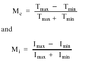
where Mc is the modulation of the chart and Mi is
the modulation of the image. The modulation transfer function of
the optical system at spatial frequency u is then defined to be

MTF curves can be either polychromatic or
monochromatic. Polychromatic curves show the effect of any
chromatic aberration that may be present. For a well-corrected
achromatic system, polychromatic MTF can be computed by weighted
averaging of monochromatic MTFs at a single image surface. MTF
can also be measured by a variety of commercially available
instruments.
The MTF curve for a perfect imaging lens is only
limited by the laws of diffraction (diffraction limited
performance). For such a system, the theoretical MTF is
calculated as follows:
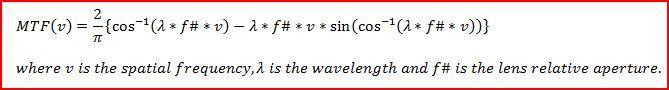
Calculate diffraction MTF using MTF wizard
To achieve this level of performance, the optical design must
be free of any aberrations, and the manufacturing process must
maintain very tight tolerances. This requires a large number
of lens elements with compensating aberrations. For most commercial
applications, the lens MTF is far from diffraction limit. The
following diagram shows the design MTF of a practical lens vs. the
diffraction limit (the black line is the diffraction limit, blue
line is the MTF on-axis and green lines off-axis at 60 deg at
tangential and saggital target orientations):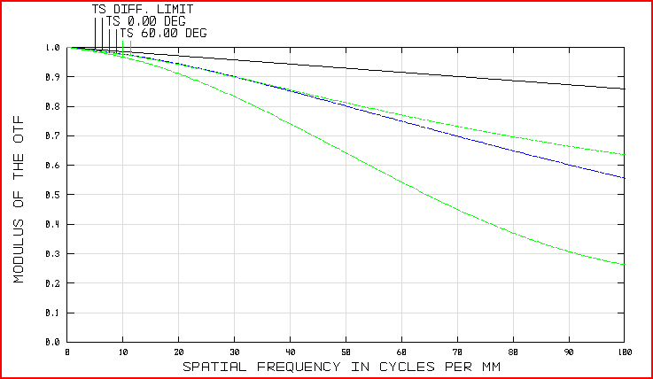
-
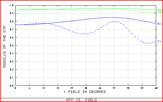
- Since a lens MTF varies with the field angle, it is often more useful to
exam the MTF at specific spatial frequencies vs. field position. This
plot shows the consistency of lens performance across the entire image
plane. It is useful to select two (a high and low) spatial
frequencies. The low frequency MTF value represents the overall
contrast of the image, and high frequency MTF represents the capability of
the lens to produce details. An example of such a plot is as follows
(green lines are MTF values at 20 cycle/mm and the blue lines at 60
cycle/mm. The solid lines are for saggital target orientation. Dash
lines for tangential orientation):
 Simulate impact of MTF to a line pair target
-
|